



广告
加载中

嘉立创深交所主板挂牌上市:股价涨146% 市值超千亿

亿邦动力 2026-08-04 10:20
亿邦动力 2026/08/04 10:20

邦小白快读

EN
全文速览

本文核心信息是嘉立创成功登陆深交所主板上市,以及其发展成果与核心优势,相关干货整理如下

1.上市核心数据:嘉立创发行价84.46元/股,上市首日股价涨幅146%,总市值达1165亿元,本次募资约46.93亿元,超出原募资计划,所有资金全部投向五大主业项目,不用于补充流动资金或还贷,项目达产后预计年新增净利润不低于5.29亿元。

2.企业发展情况:嘉立创2006年从深圳华强北一米柜台起步,目前已经成长为覆盖电子设计到制造全链条的产业互联网平台,2025年营收突破百亿元,2023-2025年营收复合增长率达23.34%,2026年第一季度营收同比增长45.29%,增长势头强劲。

3.核心竞争力:聚焦PCB小批量打样赛道,通过技术降本,把打样成本从数千元降至数十元,交付最快压缩至12小时,自研EDA软件累计注册用户超658万,全平台注册用户超950万。

本文透露了电子制造服务领域的品牌发展路径、行业趋势与可借鉴经验,相关干货整理如下

1.产业与消费趋势:全球PCB市场持续增长,AI算力基础设施建设带动高端PCB需求爆发,2026-2028年全球AI领域PCB市场规模年增速均超80%,AI硬件、商业航天等新兴行业发展,带动小批量快速验证的一站式服务需求持续提升。

2.品牌差异化定位经验:避开传统头部大厂扎堆的大批量PCB订单赛道,聚焦小批量样板细分市场,通过垂直整合从设计到制造的全产业链,打造一站式服务能力,构建了近千万工程师的用户生态,形成了差异化竞争力。

3.品牌增长与资本经验:吸引建滔、宁德时代等产业链头部企业参与战略配售,印证了自身的产业链基础设施价值,上市募资全部投入主业扩产升级,推动收入结构向高附加值的PCBA、机械产业链优化,业务协同效应持续增强,毛利率高于行业均值。

本文披露了电子产业链领域的新增增长机会、可借鉴商业模式与风险提示,相关干货整理如下

1.市场机会:PCB行业整体持续增长,AI带动高端PCB需求爆发,小批量样板赛道、PCBA、机械产业链服务增速远超传统PCB业务,2025年嘉立创境外收入同比增长44.98%,海外市场增长空间较大,新兴硬件创新对一站式小批量验证需求旺盛,蓝海市场特征明显。

2.可借鉴的商业模式:聚焦长尾小批量订单需求,通过数字化手段整合全链条服务,自研智能拼板算法整合不同客户订单拼板生产,大幅降本提效,把PCB打样成本从数千元降至数十元,交付周期从数周压缩至最快12小时,精准匹配客户需求形成竞争力。

3.风险与机会提示:当前PCB行业集中度低,传统赛道竞争激烈,传统模式毛利率较低,卖家需要找准差异化定位,向高附加值业务延伸,依托数字化提升运营效率才能获得更高收益,嘉立创上市扩产后也为上下游卖家带来更多合作机会。

本文对电子制造工厂把握市场需求、推进数字化转型、拓展商业机会提供了明确参考,相关干货整理如下

1.产品生产与设计需求变化:AI服务器、高速交换机等算力设备发展,带动高频高速、高多层等高端PCB需求持续放量,下游硬件创新迭代加快,催生大量多品种、小批量、短交期的订单,对生产柔性化的要求大幅提升。

2.商业合作机会:嘉立创本次上市募资全部投向主业,计划建设高多层PCB产线、PCBA智能产线、智能元器件中心等多个项目,需要产业链上下游工厂配合,宁德时代、建滔等不同环节头部企业都参与了嘉立创的战略配售,产业链协同合作的空间较大。

3.数字化转型启示:嘉立创通过自建五大数字化生产基地,自研智能算法整合不同订单生产,实现了柔性化生产降本提效,垂直整合全产业链减少流通环节成本,这种模式为传统电子工厂转型提供了可借鉴的路径,同时自研工业软件也能帮助工厂积累用户、提升粘性。

本文梳理了电子产业服务领域的行业趋势、客户痛点与成熟解决方案,相关干货整理如下

1.行业发展趋势:电子产业链服务正在向全链条一站式方向发展,长尾小批量需求随硬件创新快速增长,本土板级EDA工业软件已经实现用户规模突破,产业互联网模式对传统流通和制造环节的改造正在加速,行业增长动能充沛。

2.行业核心客户痛点:传统电子元器件流通环节集中度极低,以人工服务为主效率低下,无法解决长尾采购零散高频、交期管理难的痛点;传统PCB生产模式下小批量打样成本高、交期长,无法匹配硬件产品高频迭代的验证需求。

3.成熟解决方案参考:以产业互联网模式搭建线上交易平台,依托大数据、人工智能优化运营,垂直整合从设计、制造到分销、装联的全链条,提供一站式服务,嘉立创通过免费开放自研EDA工具积累了超658万注册用户,形成了稳定的用户生态壁垒,多业务协同也有效提升了客户留存和盈利能力。

本文介绍了电子产业互联网平台的发展路径、行业需求与运营经验,相关干货整理如下

1.产业对平台的核心需求:电子产业链呈现上游集中、下游极度分散的特征,存在大量长尾零散需求,传统渠道效率低下,客户需要平台整合全链条资源,提供一站式服务,降低中小硬件创新者的生产采购门槛。

2.平台运营可借鉴经验:嘉立创选择差异化定位,避开传统大厂优势的大批量订单赛道,聚焦小批量样板市场,走自营自建路线,自建生产仓储基地和线上自助下单系统,依托数字化技术实现柔性生产,通过智能算法降本提效,同时开放自研EDA工具积累海量用户,形成了封闭的用户生态。

3.平台融资与资源整合经验:嘉立创上市过程中吸引了建滔、宁德时代、康冠科技等全产业链不同环节的头部企业参与战略配售,既获得了资本认可,也绑定了产业链核心资源,这种模式值得同类平台参考,同时平台需要清晰的差异化定位,才能在分散的市场中站稳脚跟。

本文呈现了电子产业互联网领域的最新产业动向、创新商业模式与待研究问题,相关干货整理如下

1.产业新动向:全球PCB行业正经历结构性升级,AI带动高端PCB需求爆发,行业增速远超过往预期,本土板级EDA软件已经实现用户规模的突破,国内产业互联网企业正在从单一环节服务向全产业链延伸整合,嘉立创作为首个全链条电子产业互联网平台上市,会加速行业整合进程。

2.创新商业模式案例:嘉立创开创了电子产业一站式基础设施服务模式,聚焦小批量样板赛道,垂直整合从EDA设计、PCB制造、元器件分销到PCBA装联的全链条,坚持自建生产基地实现自营,精准匹配了新兴硬件创新小批量高频验证的需求,解决了传统行业效率低下的痛点。

3.待研究的行业问题:当前PCB行业整体集中度仍然较低,电子元器件流通环节整合度仍有很大提升空间,本土高端EDA技术仍待突破,这种一站式全链条模式的规模化增长潜力还有待观察,该模式已经验证了可持续盈利,规模效应下净利润复合增速高于营收,为产业互联网盈利模式提供了新的研究样本。

返回默认

声明:快读内容全程由AI生成,请注意甄别信息。如您发现问题,请发送邮件至 run@ebrun.com 。

我是 品牌商 卖家 工厂 服务商 平台商 研究者 帮我再读一遍。

Quick Summary

This article shares key takeaways from JLC's recent IPO on the Shenzhen Stock Exchange main board, including its growth achievements and core advantages:

1. Core IPO data: JLC priced its offering at RMB 84.46 per share, and its share price jumped 146% on the first trading day, pushing its total market capitalization to RMB 116.5 billion. The company raised approximately RMB 4.693 billion, exceeding its original fundraising target. All proceeds will be allocated to five core business projects, with none earmarked for working capital replenishment or debt repayment. The projects are expected to add no less than RMB 529 million in annual net profit once fully operational.

2. Company growth trajectory: Founded in 2006 starting from a 1-meter counter in Shenzhen's Huaqiangbei electronics district, JLC has grown into an industrial internet platform covering the entire value chain from electronic design to manufacturing. Its revenue surpassed RMB 10 billion in 2025, with a 23.34% compound annual growth rate (CAGR) from 2023 to 2025. Revenue grew 45.29% year-over-year in Q1 2026, indicating strong ongoing momentum.

3. Core competitive strengths: Focusing on the small-batch PCB prototyping niche, JLC leverages technology to cut prototyping costs from thousands of RMB to just dozens of RMB, and reduces delivery lead time to as little as 12 hours. Its self-developed EDA software has accumulated over 6.58 million registered users, and total registered users across the platform exceed 9.5 million.

This article outlines development paths, industry trends and actionable lessons for brands in the electronic manufacturing services sector:

1. Industrial and consumer trends: The global PCB market continues to expand. AI computing infrastructure construction is driving explosive growth in demand for high-end PCBs, with the global AI PCB market projected to grow at over 80% annually from 2026 to 2028. Growth in emerging sectors such as AI hardware and commercial space is also steadily boosting demand for one-stop services for fast, small-batch product validation.

2. Lessons for differentiated brand positioning: JLC avoided the mass-volume PCB segment dominated by large incumbents, and instead focused on the small-batch prototype niche. By vertically integrating the entire industry chain from design to manufacturing to build out one-stop service capabilities, it has built a user ecosystem of nearly 10 million engineers, forming strong differentiated competitive advantages.

3. Lessons for brand growth and capital strategy: JLC attracted strategic cornerstone investments from leading industry players including Kingboard Copper Foil and CATL, confirming its value as an infrastructure player in the electronics supply chain. All IPO proceeds will be invested in core business expansion and upgrading, to optimize its revenue mix toward higher-value-added PCBA and mechanical industry chain services. This continues to strengthen business synergies and supports gross margins above the industry average.

This article outlines new growth opportunities, replicable business models, and risk notes for players in the electronics supply chain:

1. Market opportunities: The overall PCB industry is growing steadily, with AI driving explosive demand for high-end PCBs. Growth rates for the small-batch prototype segment, PCBA, and mechanical industry chain services far outpace that of traditional PCB business. JLC's overseas revenue grew 44.98% year-over-year in 2025, pointing to significant untapped growth potential in international markets. Emerging hardware innovation has created strong, unmet demand for one-stop small-batch validation services, making this a clear blue ocean market.

2. Replicable business model: By focusing on long-tail small-batch order demand and integrating end-to-end services via digital tools, JLC developed self-owned intelligent panelization algorithms to combine orders from different customers for shared production, delivering major cost and efficiency improvements. This model cut PCB prototyping costs from thousands of RMB to dozens of RMB, and reduced lead times from weeks to as little as 12 hours, building competitive advantage through precise customer demand matching.

3. Risk and opportunity notes: The PCB industry remains highly fragmented, with fierce competition and low gross margins in traditional segments. Sellers must target a clear differentiated position, expand into higher-value-added businesses, and improve operational efficiency through digitalization to achieve higher returns. JLC's post-IPO expansion will also create new cooperation opportunities for upstream and downstream sellers.

This article provides clear actionable insights for electronics manufacturing factories on capturing market demand, advancing digital transformation, and expanding business opportunities:

1. Shifts in production and design demand: Growth of computing hardware such as AI servers and high-speed switches is driving sustained strong demand for high-end PCBs including high-frequency, high-speed and high-multilayer products. Faster iteration of downstream hardware innovation has generated large volumes of multi-variety, small-batch, short-lead-time orders, significantly raising requirements for production flexibility.

2. Business cooperation opportunities: All of JLC's IPO proceeds will be invested in core business expansion, including plans to build high-multilayer PCB production lines, intelligent PCBA production lines, and intelligent component centers. These projects require cooperation from upstream and downstream factories along the supply chain. Leading players across different supply chain segments including CATL and Kingboard have already participated in JLC's strategic private placement, highlighting significant room for industry-wide collaborative development.

3. Insights for digital transformation: JLC built five self-operated digital production bases and uses self-developed intelligent algorithms to consolidate orders from different customers for flexible production, delivering both cost reduction and efficiency gains. Its vertical integration of the entire industry chain also cuts intermediate circulation costs. This model provides a proven path for traditional electronics factories to transform, while developing self-owned industrial software also helps factories accumulate users and improve customer stickiness.

This article organizes industry trends, core customer pain points and proven solutions for the electronics industry services sector:

1. Industry development trends: Electronics supply chain services are shifting toward end-to-end one-stop offerings. Long-tail small-batch demand is growing rapidly alongside hardware innovation. Domestic board-level EDA industrial software has already achieved breakthrough user scale growth, and industrial internet-based transformation of traditional manufacturing and distribution links is accelerating, creating strong industry growth momentum.

2. Core customer pain points in the industry: Traditional electronics component distribution is highly fragmented, relies heavily on manual labor, and operates at low efficiency. It cannot solve the pain points of fragmented, high-frequency long-tail procurement and difficult lead time management. Under traditional PCB production models, small-batch prototyping is costly and has long lead times, which cannot match the validation requirements of the fast iteration cycles of modern hardware products.

3. Reference for proven solutions: Build an online trading platform via the industrial internet model, optimize operations with big data and artificial intelligence, and vertically integrate the entire value chain from design, manufacturing, distribution to assembly to deliver one-stop services. JLC accumulated more than 6.58 million registered users by opening its self-developed EDA tool for free, forming a stable user ecosystem barrier. Multi-business synergy also effectively improves customer retention and profitability.

This article introduces development paths, industry demand and operational experience for electronic industrial internet platforms:

1. Core industry demand for platforms: The electronics supply chain features concentrated upstream and highly fragmented downstream markets, with large volumes of long-tail fragmented demand. Traditional distribution channels operate at low efficiency, so customers need platforms to integrate end-to-end resources and deliver one-stop services to lower production and procurement barriers for small and mid-sized hardware innovators.

2. Actionable operational lessons for platforms: JLC adopted a clear differentiated positioning, avoiding the mass-volume order segment dominated by large incumbents to focus on the small-batch prototype market. It pursued a self-operated, vertically integrated strategy, building its own production and warehousing facilities and an online self-service ordering system, enabling flexible production via digital technology and cutting costs and boosting efficiency with intelligent algorithms. It also accumulated massive user traction by opening its self-developed EDA tool, forming a closed user ecosystem.

3. Lessons for financing and resource integration: During its IPO process, JLC attracted strategic cornerstone investments from leading players across all segments of the supply chain, including Kingboard, CATL and KTC. This not only secured capital endorsement but also locked in core supply chain resources, making this a model worth replicating for peer platforms. The case also highlights that a clear differentiated positioning is required for platforms to gain a foothold in highly fragmented markets.

This article presents the latest industry developments, innovative business models and open research questions in the electronic industrial internet sector:

1. New industry developments: The global PCB industry is undergoing structural upgrading, with AI driving explosive demand for high-end PCB that has pushed industry growth far past earlier expectations. Domestic board-level EDA software has already achieved breakthrough user scale growth, and Chinese industrial internet firms are expanding from single-link services to end-to-end industry chain integration. As the first end-to-end electronic industrial internet platform to go public, JLC's listing will accelerate industry consolidation.

2. A case study in innovative business model: JLC has pioneered a one-stop infrastructure service model for the electronics industry, focusing on the small-batch prototype niche. It vertically integrates the entire value chain from EDA design, PCB manufacturing, component distribution to PCBA assembly, and insists on self-operation through owned production bases. This model precisely matches the small-batch, high-frequency validation demand of emerging hardware innovation, and solves the efficiency pain points of the traditional industry.

3. Open industry research questions: The overall PCB industry remains highly fragmented, and there is still significant room for consolidation in the electronics component distribution segment. Domestic high-end EDA technology still requires further breakthroughs. The large-scale growth potential of this end-to-end one-stop model remains to be observed. That said, the model has already proven it can deliver sustainable profitability, with net profit CAGR outpacing revenue CAGR as scale effects kick in, providing a valuable new research case for industrial internet profitability models.

Disclaimer: The "Quick Summary" content is entirely generated by AI. Please exercise discretion when interpreting the information. For issues or corrections, please email run@ebrun.com .

I am a Brand Seller Factory Service Provider Marketplace Seller Researcher Read it again.

【亿邦原创】8月4日,深圳嘉立创科技集团股份有限公司(证券简称"嘉立创",证券代码001232)正式在深圳证券交易所主板挂牌上市。本次发行价84.46元/股,公开发行5556万股,募集资金总额约46.93亿元,发行后市盈率38.19倍。

开盘之后,嘉立创股价涨幅146%,总市值达到1165亿元。

作为电子产业一站式基础设施服务提供商,嘉立创以102.32亿元的年营收、950万注册用户和年2100万笔订单,成为A股市场首个集EDA工业软件、PCB制造、电子元器件分销、PCBA及机械产业链服务于一体的产业互联网平台型上市公司。

一、三年闯关上市,超额募资46.93亿元

嘉立创的A股之路始于2023年。2023年6月30日,深交所正式受理嘉立创的主板IPO申请,融资金额66.7亿元。一个月后(7月31日),深交所发出第一轮审核问询函,公司进入问询阶段。此后,因财务资料过期需要补充更新,审核程序多次中止与恢复,IPO进程一度在问询阶段停留逾两年半。

在此期间,嘉立创经历了多轮财务资料更新与问询回复。2024年3月,公司对外披露首轮审核问询函回复。招股书显示,2021年、2022年,嘉立创分别实施现金分红2.7亿元和4亿元,这一事项曾引发深交所重点关注,要求说明现金分红的必要性与合理性。公司回复称,报告期内现金流量和资产负债情况良好,分红后财务状况保持稳健。

2026年,IPO进程明显提速。5月12日,嘉立创上市申请获得深交所上市审核委员会2026年第22次会议审议通过,当日提交注册;6月2日,中国证监会同意注册(证监许可〔2026〕1306号),注册生效;7月16日,嘉立创披露招股意向书,正式启动发行;7月21日,完成初步询价,确定发行价84.46元/股;7月24日,网上网下同步申购。

嘉立创本次发行最终募资约46.93亿元,扣除发行费用后净额约44.48亿元,超出原计划42亿元的募资需求。战略配售方面,初始战略配售数量为1111.20万股,最终战略投资者获配994.5531万股,占发行总量的17.90%。值得关注的是,获配名单中出现了建滔(全球覆铜板龙头)、宁德时代(新能源产业链核心龙头)、康冠科技(智能终端制造企业)等不同环节的头部企业,侧面印证了嘉立创在硬件产业链中的基础设施价值。

本次募集资金将全部投向主业,不用于补充流动资金或偿还贷款,五大项目包括:① 高多层印制线路板产线建设项目;②PCBA智能产线建设项目;③ 研发中心及信息化升级项目;④ 智能电子元器件中心及产品线扩充项目;⑤ 机械产业链产线建设项目。据招股文件,募投项目达产后预计每年新增净利润不低于5.29亿元。

二、三年复合增长超23%,营收突破百亿

嘉立创由丁会、袁江涛、丁会响三位创始人在2006年从深圳华强北一间一米柜台起步,开拓PCB小批量打样赛道。三人签署共同控制协议,合计直接和间接持有公司87.5%的股份,为实际控制人。

嘉立创自定位为"业内领先、具有行业变革意义的电子产业一站式基础设施服务提供商",以"助力全球硬件创新"为使命,业务覆盖从设计到制造的全链条:

电子产业链服务:包括EDA/CAM工业软件(嘉立创EDA、CAM、DFM、ECAD等)、印制电路板(PCB)制造、电子元器件购销(立创商城)、电子装联(PCBA)及激光钢网等配套服务。

机械产业链服务:包括FA机械/电气零部件商城、3D打印、CNC智造、钣金加工等,满足硬件产品从电路功能验证到外壳、支架、传动等结构验证的延伸需求。

工业软件:自研板级EDA工业软件"嘉立创EDA"累计注册用户已超658万人,促成设计硬件项目超4300万个,在用户规模、功能设计和研发投入等方面处于国内板级EDA领域领先位置。

嘉立创依托自建的下单网站和自有生产仓储基地,在广东省珠海、惠州、韶关及江西吉安、江苏淮安等地建立了总面积近1800亩的五大现代化数字生产基地和两大智能电子元器件仓储基地,实现了业务条线的垂直化整合和产业链的纵向延伸。

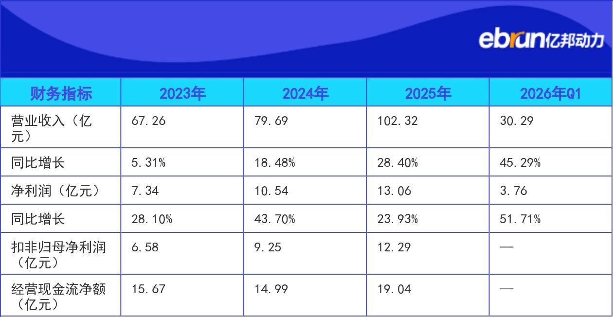
财务指标 2023年 2024年 2025年 2026年Q1
营业收入(亿元) 67.26 79.69 102.32 30.29
同比增长 5.31% 18.48% 28.40% 45.29%
净利润(亿元) 7.34 10.54 13.06 3.76
同比增长 28.10% 43.70% 23.93% 51.71%
扣非归母净利润(亿元) 6.58 9.25 12.29
经营现金流净额(亿元) 15.67 14.99 19.04

2023年至2025年,嘉立创营收复合增长率达23.34%,净利润复合增长率达33.45%,显著高于营收增速,规模效应持续显现。2025年营收首次突破百亿元,高增长势头已延续至2026年,第一季度营收和净利润分别同比增长45.29%和51.71%。

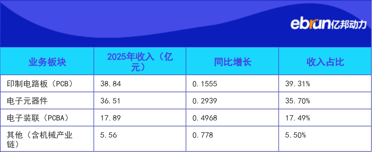
业务板块 2025年收入(亿元) 同比增长 收入占比
印制电路板(PCB) 38.84 0.1555 39.31%
电子元器件 36.51 0.2939 35.70%
电子装联(PCBA) 17.89 0.4968 17.49%
其他(含机械产业链) 5.56 0.778 5.50%

值得注意的是,PCB业务在收入结构中的占比已降至四成以下,而PCBA和机械产业链服务的增速远超传统业务,收入结构正向更高附加值方向优化。2025年,PCBA业务带动实现PCB收入4.69亿元,对当期PCB收入增长的贡献比例达28.95%,业务协同效应持续加强。在机械产业链服务中,3D打印、CNC制造和FA业务合计实现收入4.33亿元。

运营数据方面,截至2025年末,嘉立创在线自助下单网站注册用户超950万,覆盖全球超180个国家和地区;付费用户超130万;全年处理订单超2100万单(同比增长19.49%)。立创商城现货库存SKU超70万,年出货订单量超390万单。2025年境外收入20.45亿元,同比增长44.98%。公司拥有员工超10000人,累计获得180项专利及285项软件著作权。

三、PCB市场超850亿美元,产业互联网重塑流通链路

印制电路板(PCB)被称为"电子产品之母",是各类电子元器件的载体和电气连接的桥梁。根据行业研究机构Prismark数据,2025年全球PCB行业产值达851.52亿美元,同比增长15.75%,增速超预期。其中,中国大陆PCB产值为489.69亿美元,占全球份额的57.5%,连续20年位居全球首位。Prismark预测,2026年全球PCB市场产值将达到957.8亿美元,同比增长12.5%;2025-2030年行业复合增速为7.7%,2030年市场规模将突破1233亿美元。

当前,AI算力基础设施建设进入高速发展期,PCB作为AI服务器、高速光模块、算力交换机的核心互联载体,正迎来结构性增长机遇。AI服务器、高速交换机等核心算力设备对高频高速、高多层、高阶HDI等高端PCB产品的需求持续放量,叠加单台AI设备的PCB价值量较传统服务器大幅提升,行业成长动能充沛。

据花旗证券2026年6月研报,2026-2028年全球AI领域的PCB市场规模有望达到1520亿元、3070亿元、5620亿元,各年增长率分别为86%、102%、83%。鹏鼎控股、深南电路、沪电股份等头部企业纷纷加大高端产线投入,行业正经历从传统多层板向HDI板、IC封装基板、高频高速板等高附加值产品的结构性升级。

全球共有近3000家PCB企业,市场集中度不高。2021年全球前十大厂商营收合计284.55亿美元,市占率约35.16%。行业竞争格局呈现清晰的金字塔型梯队:鹏鼎控股连续九年位居全球PCB营收第一,深南电路与沪电股份在通信、AI服务器等高端领域构筑深厚技术壁垒,东山精密深度绑定海外大客户为全球FPC巨头。

从需求结构看,PCB可分为样板、小批量板和中大批量板。样板和小批量板订单数量多、金额小、种类复杂、交期要求短,对生产柔性化要求高;而中大批量板订单数量少、金额大、周期长,对生产稳定性和良率要求高。传统大厂如鹏鼎控股、深南电路主攻大批量订单,而嘉立创则聚焦样板和小批量市场,实现"一片起订",通过自研智能拼板算法将不同客户的订单组合生产,将PCB单次打样成本从数千元降至数十元,交付周期从数周压缩至最快12小时。2025年,嘉立创PCB业务毛利率达28.09%,高于行业可比公司均值。

在电子元器件流通环节,上游集中、下游分散、品类繁杂是核心特征。约99%的下游制造商通过分销商渠道采购,行业集中度极低——2021年国内前三大分销商市占率低于5%,前十大的市占率低于10%。传统流通渠道以人工服务为主、效率较低,而以嘉立创(立创商城)、华强电子网、云汉芯城为代表的产业互联网B2B商城,通过线上交易以及大数据与人工智能支持,有效解决了长尾采购需求零散高频、交期管理难、采购效率低下等行业痛点。

值得注意的是,PCB设计、PCB制造、电子元器件分销、电子装联的需求是相互关联的。华强电子网、嘉立创、云汉芯城等具备互联网数字化能力的企业,虽然业务侧重点不同——嘉立创业务线最长,覆盖PCB设计、PCB制造、电子元器件分销、电子装联全链条;云汉芯城和华强电子网主要集中于电子元器件分销——但都在依托线上交易积累的大数据优势向全产业链延伸,最终目标是实现一站式服务。

嘉立创的差异化竞争力在于,它是唯一一家同时拥有近千万工程师用户生态、覆盖从设计到制造全链条、自建生产基地实现产品自营制造的硬件创新平台型企业。在AI硬件、具身智能、商业航天等新兴行业加速落地的背景下,这种"一站式"服务模式与硬件产品高频迭代、小批量验证的研发需求形成了高度匹配。

文章来源:亿邦动力

广告
微信
朋友圈

FAQ回顾

嘉立创是一家什么企业?

嘉立创是电子产业一站式基础设施服务提供商,业务覆盖EDA工业软件、PCB制造、电子元器件分销、PCBA及机械产业链服务,是A股首个集上述业务于一体的产业互联网平台型上市公司,2025年营收达102.32亿元,注册用户超950万。

嘉立创上市后的市值有多少?

2026年8月4日嘉立创正式在深交所主板挂牌上市,发行价为84.46元/股,开盘后股价涨幅达146%,总市值达到1165亿元,本次公开发行募资总额约46.93亿元,募资将全部投向主业相关五大项目。

PCB行业未来的发展前景如何?

根据Prismark预测,2026年全球PCB市场产值将达957.8亿美元,2025-2030年行业复合增速为7.7%,2030年市场规模将突破1233亿美元。AI算力基础设施建设驱动高端PCB需求放量,行业正朝高附加值产品方向结构性升级。

嘉立创的核心竞争优势是什么?

嘉立创的差异化竞争力在于同时拥有近千万工程师用户生态,覆盖从设计到制造全链条,自建生产基地实现产品自营制造,其一站式服务模式与硬件产品高频迭代、小批量验证的研发需求高度匹配,2025年PCB业务毛利率高于行业可比公司均值。

这么好看,分享一下?

朋友圈 分享

APP内打开

+1
+1
微信好友 朋友圈 新浪微博 QQ空间
关闭
收藏成功
发送
/140 0